
MIT scientists have engineered a groundbreaking photonic processor that harnesses light waves instead of electrical currents, delivering unprecedented energy efficiency for artificial intelligence computations. This innovative optical chip could transform how massive neural networks are processed, performing calculations millions of times more efficiently than conventional computer systems.
Neural networks, the machine-learning frameworks powering applications from autonomous vehicles to medical diagnostics and natural language processing, require enormous computational resources. Traditional electronic processors struggle with the energy demands of these complex systems. However, optical neural networks utilizing light-based computations offer significantly faster and more efficient alternatives to their electronic counterparts.
As both conventional and optical neural networks increase in complexity, their power consumption skyrockets. To address this challenge, leading technology companies including Google, IBM, and Tesla have developed specialized AI accelerators—chips designed specifically to enhance the speed and efficiency of neural network training and deployment.
For electronic chips, including most AI accelerators, fundamental physical laws impose a theoretical minimum energy consumption threshold. Recently, MIT researchers have pioneered photonic accelerators for optical neural networks. While these chips demonstrate orders of magnitude improvement in efficiency, their reliance on bulky optical components has limited their application to relatively small neural networks.
In a groundbreaking study published in Physical Review X, MIT researchers detail a novel photonic accelerator incorporating compact optical components and advanced optical signal-processing techniques. This innovation dramatically reduces both power requirements and physical footprint, enabling the chip to scale to neural networks orders of magnitude larger than previous photonic processors.
Simulated neural network training using the MNIST image-classification dataset indicates that the accelerator can theoretically operate more than 10 million times below the energy-consumption limit of traditional electronic accelerators and approximately 1,000 times below the limit of existing photonic accelerators. The research team is currently developing a physical prototype to validate these remarkable results experimentally.
"The technology community is actively seeking solutions that can突破 the fundamental energy consumption barriers in computing," explains Ryan Hamerly, a postdoc in the Research Laboratory of Electronics. "While photonic accelerators show tremendous promise, our primary goal was to develop a photonic processor capable of scaling to accommodate large neural networks."
Practical implementations of this technology could revolutionize energy efficiency in data centers worldwide. "We're witnessing exponential growth in demand for data center resources dedicated to running large neural networks, and this demand is becoming increasingly challenging to meet computationally," notes co-author Alexander Sludds, a graduate student in the Research Laboratory of Electronics. "Our objective is to address this computational demand with specialized neural network hardware that overcomes the critical bottlenecks of energy consumption and latency."
Joining Sludds and Hamerly on the research paper are: co-author Liane Bernstein, an RLE graduate student; Marin Soljacic, an MIT professor of physics; and Dirk Englund, an MIT associate professor of electrical engineering and computer science, a researcher in RLE, and head of the Quantum Photonics Laboratory.
Revolutionary Compact Architecture
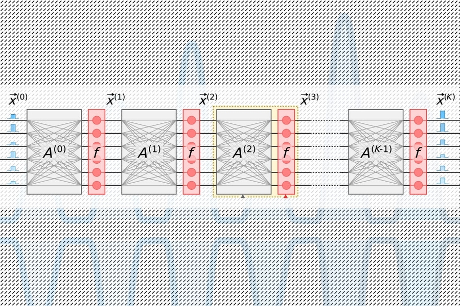
Neural networks process information through multiple computational layers containing interconnected nodes, or "neurons," to identify patterns in data. Each neuron receives input from upstream connections and computes an output signal transmitted to downstream neurons. Every input is assigned a "weight"—a value reflecting its relative importance compared to other inputs. As data propagates through successive layers, the network progressively learns to recognize more complex patterns, ultimately generating predictions in the output layer based on calculations performed throughout the network.
All AI accelerators aim to minimize the energy required for processing and moving data during a specific linear algebra operation in neural networks known as "matrix multiplication." In this process, neurons and weights are encoded into separate tables of rows and columns and then combined to calculate outputs.
Conventional photonic accelerators employ pulsed lasers encoded with neuron information, which travel through waveguides and beam splitters. The resulting optical signals enter a grid of square optical components called "Mach-Zehnder interferometers," programmed to perform matrix multiplication. These interferometers, encoded with weight information, utilize signal-interference techniques to process optical signals and weight values, computing outputs for each neuron. However, a significant scaling challenge emerges: each neuron requires one waveguide, and each weight necessitates one interferometer. Since the number of weights increases quadratically with the number of neurons, these interferometers consume substantial chip space.
"You quickly realize that the number of input neurons cannot exceed approximately 100, because you simply cannot fit that many components on the chip," Hamerly explains. "If your photonic accelerator cannot process more than 100 neurons per layer, implementing large neural networks within that architecture becomes impractical."
The researchers' chip employs a more compact, energy-efficient "optoelectronic" approach that encodes data using optical signals but utilizes "balanced homodyne detection" for matrix multiplication. This technique generates a measurable electrical signal after calculating the product of the amplitudes (wave heights) of two optical signals.
Light pulses encoded with input and output neuron information for each neural network layer—essential for network training—travel through a single channel. Separate pulses encoded with entire rows of weight information from the matrix multiplication table flow through individual channels. Optical signals carrying neuron and weight data distribute to a grid of homodyne photodetectors. These photodetectors calculate output values for each neuron using signal amplitudes. Each detector then feeds an electrical output signal for each neuron into a modulator, which converts the signal back into a light pulse. This optical signal becomes the input for the subsequent layer, continuing the process throughout the network.
This architecture requires only one channel per input and output neuron and only as many homodyne photodetectors as there are neurons, not weights. Since there are always significantly fewer neurons than weights, this approach saves considerable space, enabling the chip to scale to neural networks with over a million neurons per layer.
Optimizing the Efficiency-Precision Balance
Photonic accelerators inherently introduce signal noise. Increasing the light input to the chip reduces noise and improves accuracy—but at the cost of efficiency. Conversely, reducing input light enhances efficiency but negatively impacts neural network performance. However, researchers identified an optimal "sweet spot" that minimizes optical power requirements while maintaining computational accuracy, as Bernstein explains.
This optimal efficiency point for AI accelerators is measured by the energy required to perform a single multiplication operation—such as those in matrix multiplication. Current traditional accelerators operate in the picojoule range (one-trillionth of a joule). Photonic accelerators operate in the attojoule range—a million times more efficient.
In their simulations, the researchers demonstrated that their photonic accelerator could achieve sub-attojoule efficiency. "There exists a minimum optical power threshold below which accuracy deteriorates," Bernstein notes. "The fundamental efficiency limit of our chip is substantially lower than traditional accelerators—and even below other photonic accelerators."

